
Consistent light for consistent results.
LED illumination, laser modules and enclosures for AOI, wafer inspection, 3D metrology and assembly, built to give the same result on every shift and every tool.
The inspection problem is getting harder
Components keep shrinking, tolerances keep tightening, and line speeds keep rising. Reflective finishes, low-contrast marks and defects inside the material are hard to see with ordinary lighting. A light source that drifts makes this worse. A small change in output can turn a pass into a fail, and the false rejects and rework that follow are hard to trace back to the light.
The fix starts with the light. If you choose the right wavelength, geometry and stability for the task, the camera sees the defect clearly and the result can be repeated.
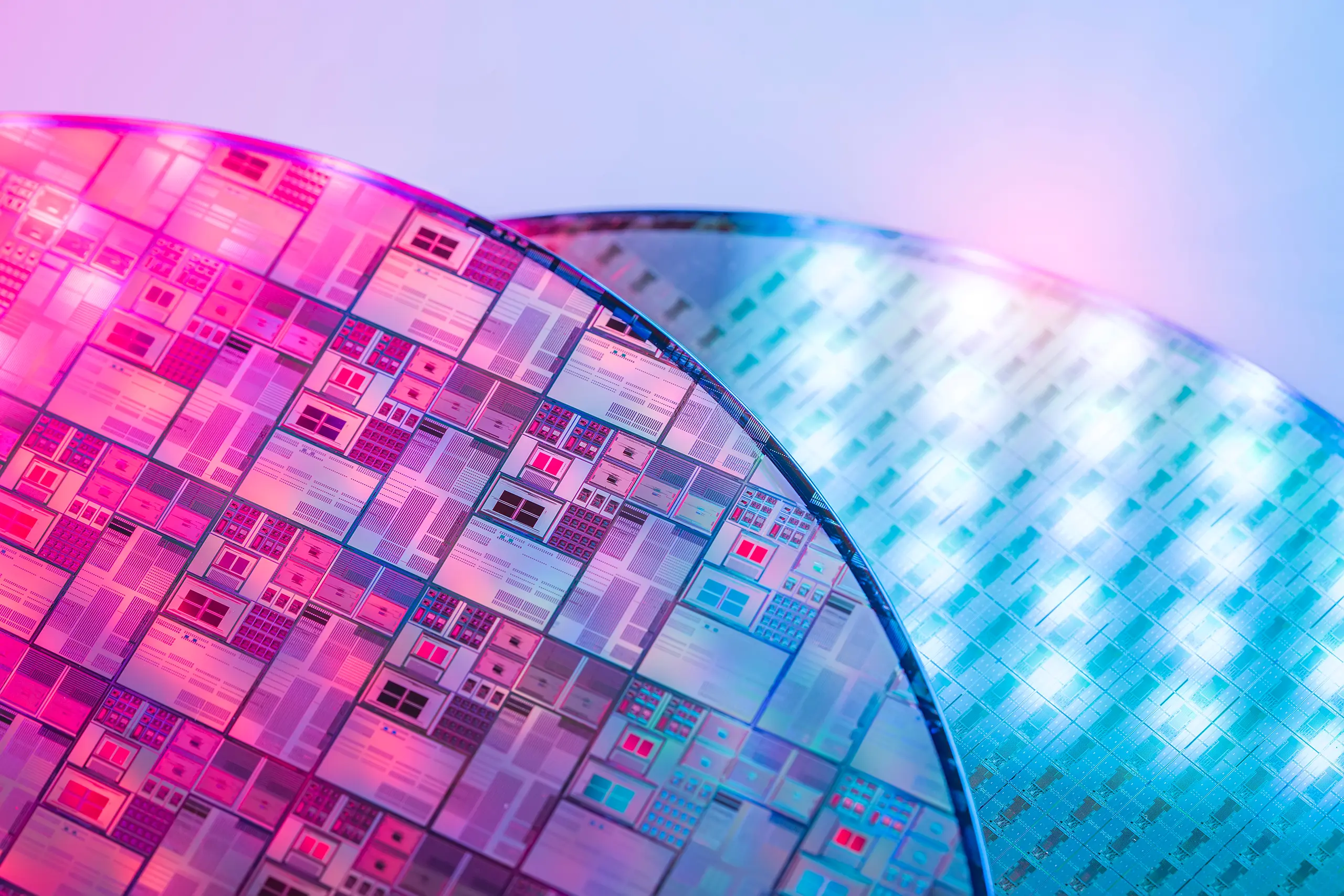
Electronics and semiconductor inspection applications
Automated optical inspection (AOI)
High-intensity ring and diffuse LED lighting for solder joint quality, lead inspection, component placement and fiducial mark identification on PCB assembly and packaging lines, with the geometry chosen to suit the joint type and board finish. UV at 365nm reveals flux residue and contamination invisible under visible wavelengths, a common requirement for conformal coating inspection and board cleanliness verification before potting.
Wafer and die inspection
Structured light and LED illumination for wafer edge detection, flatness measurement, surface defect mapping, contamination detection and die-level inspection. Scratches, chipping, edge defects, thin-film peeling and surface particles are resolved at sub-micron scale. The best wavelength depends on the substrate, because silicon, compound semiconductors and III-V materials each reflect and absorb light differently.
PCB traceability and marking verification
LED illumination for reading laser-marked 2D codes, datamatrix and QR codes on PCBs and assemblies. Dark-field LED lighting brings out low-contrast marks on bare copper, tin and ENIG finishes where direct lighting causes specular glare. Codes can be verified inline without slowing the line.
Enclosures for inspection equipment
Exaktera enclosures protect cameras, lenses, lighting and lasers so inspection results stay consistent over the working life of the equipment. Stainless steel camera enclosures with IP69K protection keep dust, moisture and cleaning agents away from the optics, and a dedicated laser enclosure system makes machine vision equipment quicker to install and align.
Wavelength, geometry and uniformity for semiconductor inspection.
Exaktera LED lighting covers the wavelengths and geometries semiconductor inspection needs: UV (365nm) for flux and contamination, dark-field for low-contrast features on PCBs and substrates, NIR for imaging through PCBs and inspecting multi-layer traces, and SWIR for making hidden material differences in silicon wafers visible. Polarisation reduces specular glare, and high-intensity pulsed operation allows short exposure times at high speed without motion blur, with output controllable frame by frame.
Stable, uniform output matters in this industry, both across the shift and from one tool to the next. A drift in intensity can push a borderline result from pass to fail and cause false rejects. Exaktera LED drive electronics hold output stable to within 0.5% over temperature.
Stable laser sources for metrology.
Exaktera laser diode assemblies and laser modules provide stable, spectrally pure sources for structured light measurement and laser triangulation in semiconductor metrology. Compact structured light modules produce uniform, narrow lines for 3D measurement. Long-term power stability and wavelength accuracy matter where measurement budgets are tight, because drift in the source can read as a measurement error and is hard to trace.
Custom configurations are available where the standard range does not cover the wavelength, light pattern or output power you need.
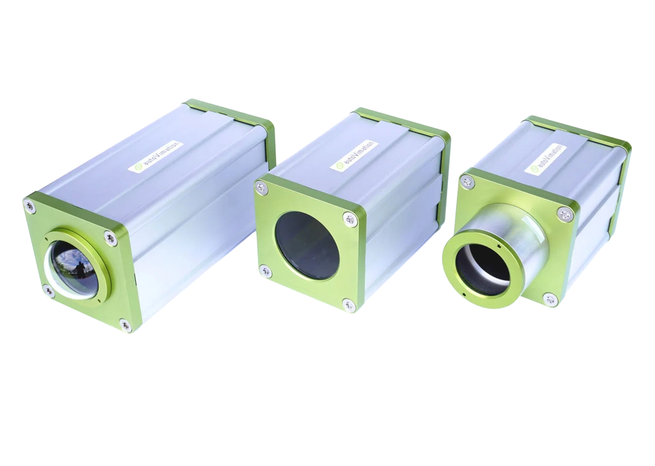
Protection for cameras, lighting and lasers on the tool.
Exaktera enclosures protect cameras, lenses, lighting and lasers so inspection results stay consistent over the working life of the equipment. Stainless steel camera enclosures with IP69K protection keep dust, moisture and cleaning agents away from the optics, and a dedicated laser enclosure system makes machine vision equipment quicker to install and align.
Each enclosure is specified around the camera, lens and lighting it will house, with the window material, mounting and cable routing chosen to suit the tool. Custom configurations are available where a standard enclosure does not fit.
Our engineers work with integrators, semiconductor equipment manufacturers and semiconductor manufacturers on illumination, laser sources and enclosures for precision inspection environments.